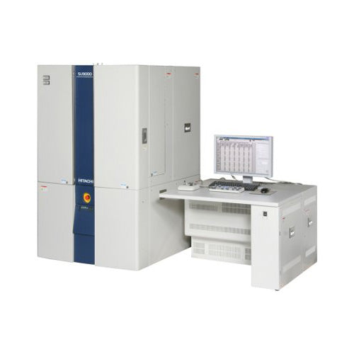
Description
The Hitachi SU9000 is an ultra-high-resolution cold field emission in-lens SEM delivering world-leading 0.4 nm SE resolution at 30 kV. Its true in-lens design positions the sample inside the objective lens pole piece gap, combined with next-generation cold FEG technology for maximum brightness and stability. The 2+2 detection system with patented Super ExB filter provides surface, compositional, and transmission imaging. As a powerful low-kV STEM with 0.34 nm resolution, EELS with 400 meV energy resolution, and simultaneous BF/DF imaging with 56 darkfield detector positions, it bridges SEM and TEM for advanced nanocharacterization of catalysts, nanomaterials, graphene, and biological specimens.
Specifications
| Manufacturer | Hitachi High-Tech |
|---|---|
| Model Name | SU9000 |
| Model Number | SU9000 |
| Accelerating Voltage Kv | 0.5, 30 |
| Electron Source | Cold FEG |
| Sem Resolution Nm 30kv | 0.4 |
| Sem Resolution Nm 1kv | 1.2 |
| Sem Resolution Nm 1kv Decel | 0.8 |
| Stem Resolution Nm | 0.34 |
| Magnification Range | 100, 3000000 |
| Routine Magnification | 1000000 |
| Detector System | 2+2 detection |
| Detector Types | Upper SE (Super ExB filter), Top BSE (HA-BSE), STEM-BF, STEM-DF (56 positions) |
| In Lens Design | Yes |
| Eds Capable | Yes |
| Eds Collection Angle Sr | 0.7 |
| Eels Capable | Yes |
| Eels Energy Resolution Mev | 400 |
| Eels Detectors | 2 |
| Eels Fps | 10000 |
| Vacuum Level | UHV |
| Sample Stage | side-entry |
| Max Sample Size Mm | 5.0 x 9.5 x 3.5 |
| Beam Deceleration | Yes |
| Diffraction Capable | Yes |
Imaging Modes
Secondary Electron
Backscattered Electron
Stem Bf
Stem Df
Low Voltage Stem
Eds Mapping
Eels
Energy Filtered Stem
Diffraction
Typical Specimens
Nanomaterials
Catalyst
Carbon Nanotubes
Graphene
Quantum Dots
Biological Immunolabeling
Semiconductor
Nanoparticles
Clinical Applications
Nanomaterial Characterization
Catalyst Research
Semiconductor Failure Analysis
Pharmaceutical Immunolabeling
Materials Science
Life Sciences