Semiconductor Wafer Surface
Semiconductor Wafer Surface
Materials ScienceSilicon wafer cross-section showing transistor gate structures
Drag & drop images here to add to this specimen
or click Upload Image aboveRelease to upload
Image Library
3 images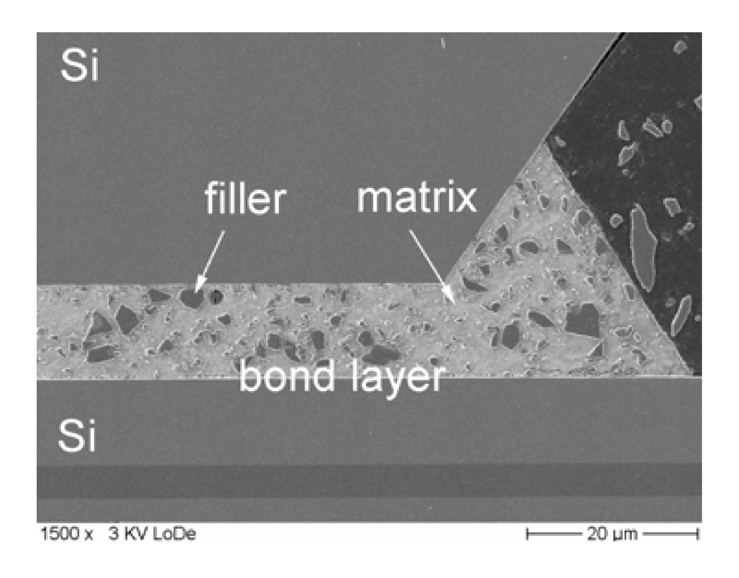
SEM cross-section of a silicon wafer showing deep reactive ion etched (DRIE) structures created by the Bosch process. The high-aspect-ratio trenches with characteristic scalloped sidewalls demonstrate precision semiconductor fabrication at the micrometer scale.
SEM cross-section — Bosch process DRIE silicon etching
Wikimedia Commons — CC BY-SA 3.0
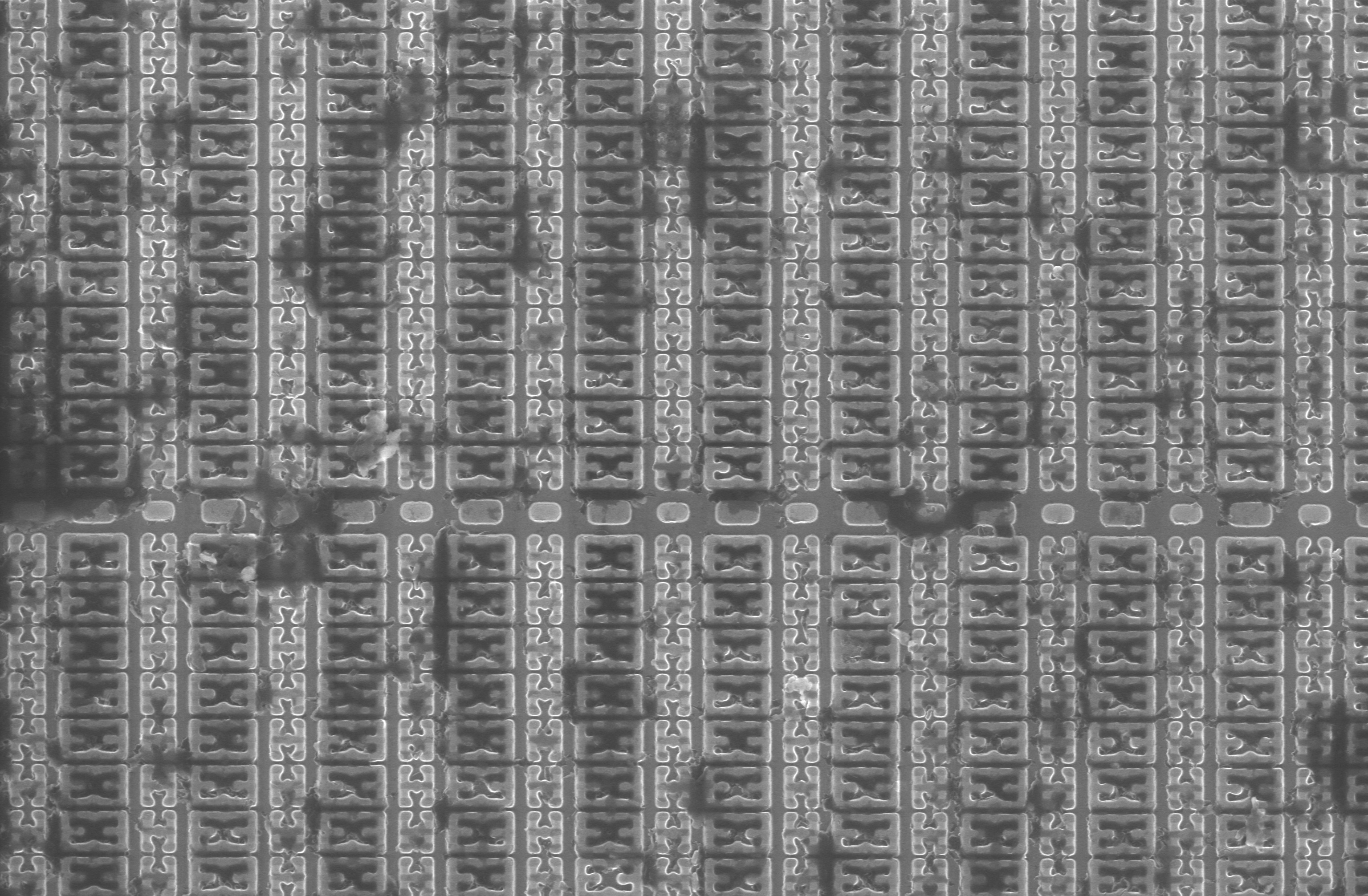
Scanning electron microscope image of an STM32F103VGT6 ARM Cortex-M3 microcontroller die showing the full IC layout including memory arrays, logic blocks, peripheral circuits, and bond pads. Manufactured on 90nm CMOS process.
Full die SEM overview — STM32 ARM microcontroller IC layout
Wikimedia Commons — CC BY-SA 3.0
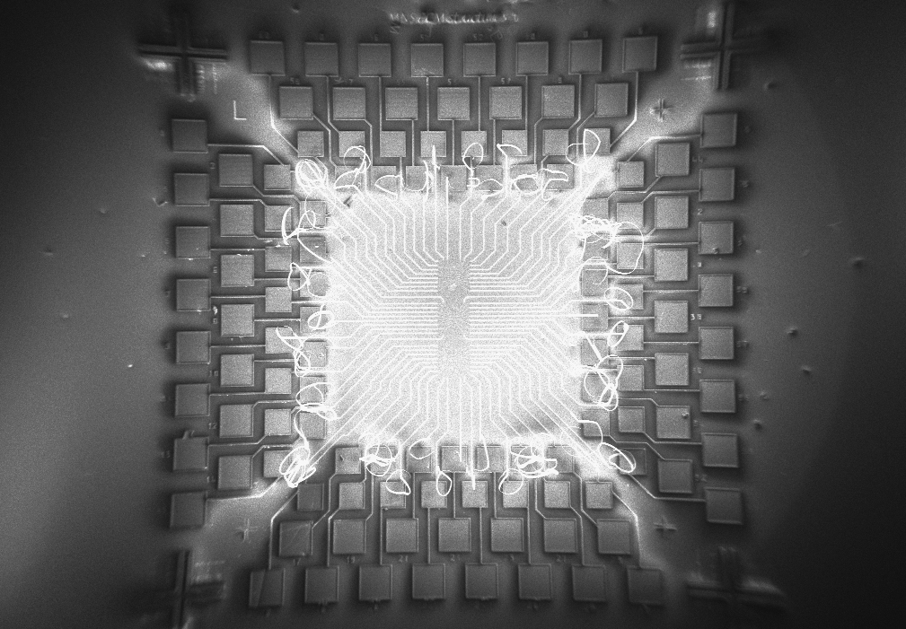
SEM image of a semiconductor die designed for carbon nanotube field-effect transistor (CNTFET) fabrication. Shows lithographically patterned electrode structures, contact pads, and nanoscale channel regions on the wafer surface.
SEM — CNTFET fabrication die with electrode patterning
Wikimedia Commons — CC BY-SA 3.0
Compatible Microscopes
| Model | Manufacturer | Type | Magnification Range | NA Max | Resolution |
|---|---|---|---|---|---|
| Dimension Icon | Bruker | Afm | -–-× | — | — nm |
| MultiMode 8 | Bruker | Spm | -–-× | — | — nm |
| SkyScan 1275 | Bruker | Micro Ct | -–-× | — | — nm |
| SkyScan 1273 | Bruker | Micro Ct | -–-× | — | — nm |
| HT7800 | Hitachi High-Tech | Tem | 200–600000× | — | — nm |
| Regulus 8200 | Hitachi High-Tech | Fe Sem | 20–2000000× | — | 0.6 nm |
| JEM-F200 | JEOL | Tem | 50–1500000× | — | — nm |
| JSM-IT800 | JEOL | Sem | 5–1000000× | — | 0.7 nm |
| JSM-7900F | JEOL | Fe Sem | 25–1000000× | — | 0.5 nm |
| nano3DX | Rigaku | X Ray Microscope | -–-× | — | — nm |
| inspeXio SMX-225CT FPD HR Plus | Shimadzu | Micro Ct | -–-× | — | — nm |
| Apreo 2 | Thermo Fisher Scientific | Fe Sem | 13–2000000× | — | 0.7 nm |
| Helios 5 UX | Thermo Fisher Scientific | Fib Sem | 55–2400000× | — | — nm |
| Xradia 520 Versa | Zeiss | X Ray Microscope | -–-× | — | — nm |
| Xradia 620 Versa | Zeiss | X Ray Microscope | -–-× | — | — nm |
| Xradia 800 Ultra | Zeiss | X Ray Microscope | -–-× | — | — nm |
Edit Image Metadata
AI Generate Image — Semiconductor Wafer Surface
Fill in the imaging criteria below. A detailed prompt will be built from your selections and sent to OpenAI to generate a realistic microscopy image.